Researchers Develop One-Atom-Thick 2D Wafers in Major Breakthrough
Semiconductors have always adapted to meet the changing needs of the devices they power. But as devices grow smaller, there are limits to the capabilities of silicon wafers. That’s why researchers are constantly on the lookout for new semiconductor materials and techniques for making them. A team of Chinese scientists made a breakthrough with so-called “2D” wafers that are just one atom thick.
The new material touts superior semiconducting properties and the team believes it could revolutionize the chip industry. Although more work is needed to turn this 2D material into viable chips, this breakthrough is an exciting step forward.
Solving the Wafer Size Problem
As silicon wafers get thinner, they offer worse voltage control, leading to excess heat generation and more energy costs when they’re turned into chips. Naturally, this poses a problem for making semiconductors that are as small as possible.
The new MoS2 material is composed of crystalline material layers just an atom thick. This gives them unique properties and allows them to vastly outperform silicon wafers of the same thickness, says study lead professor Liu Kaihui of Peking University. In an exclusive interview with the South China Morning Post, Liu said of the team’s achievement, “We proved to the industry that this is scientifically feasible and instilled confidence. If there are industrial demands in the future, progress in this field will advance by leaps and bounds.”
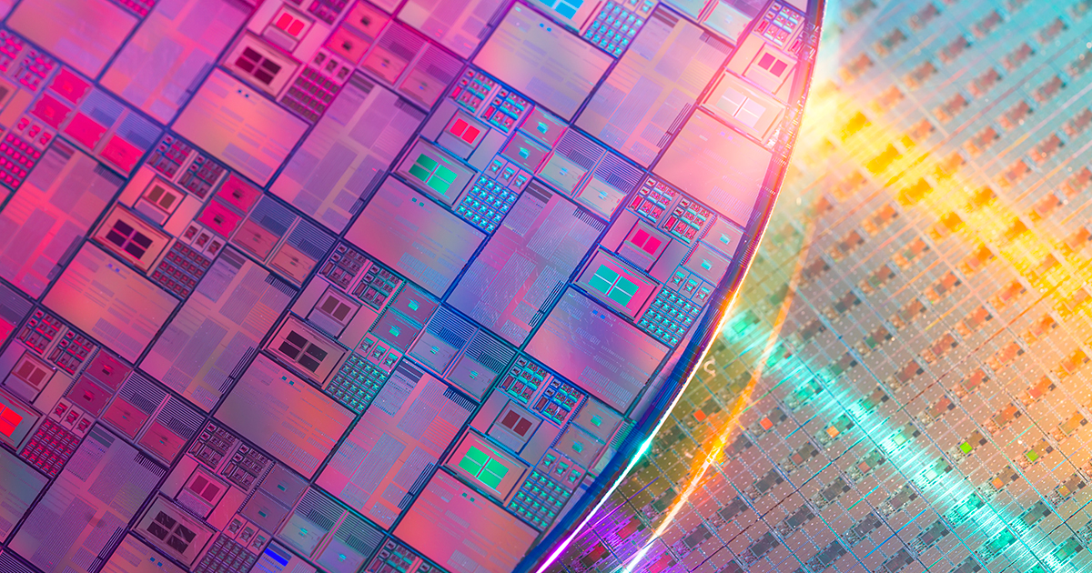
It goes without saying that producing 12-inch wafers with materials an atom thick is a challenge. Scientists typically struggle to keep the layers uniform as the diameter of the wafer gets wider. Although two-inch wafers have been successfully produced in the past, roughly 60% of today’s chip market relies on 12-inch wafers. Any 2D material would need to be scaled up to remain compatible with existing machinery and designs.
To solve the size problem, the team ditched traditional point-to-surface methods and developed what it calls a surface-to-surface supply method. Researchers then designed their own equipment to support the new method.
Liu says the team can now produce 10,000 of the 2D wafers per machine every year. Notably, Liu also notes the method is capable of producing wafers larger than 12 inches should they be necessary. The new surface-to-surface method is a massive leap forward, allowing for both precise and efficient manufacturing.
Waiting in the Wings
A 2D wafer isn’t ready to perform as a fully functioning chip on its own, though. Chip design and photolithography and deposition are still needed. Given the novelty of 2D materials, manufacturing techniques haven’t quite caught up and further research into manufacturing with them is needed. Fortunately, those strides are already being taken.
Liu says, “Leading semiconductor companies like TSMC, Intel, and Samsung are investing heavily in research and development. There’s a transitional phase for two-dimensional semiconductors from laboratory to industrial application.”
China is also researching 2D chip technology. However, Liu notes that 2D semiconductors likely won’t begin playing a vital role in the future until the limitations of silicon chips start causing significant problems.
As it stands, silicon still reigns supreme. Chipmakers are finding plenty of new ways to advance their designs and squeeze more power from existing technology. Innovations such as chiplets show that even older technology can be made more efficient with a creative approach.
But 2D semiconductor technology is worth monitoring. This is an exciting field with new breakthroughs being made often. In the short term, 2D chips could work alongside traditional silicon to give our devices a boost and make them operate more efficiently. While no one can predict the future, this technology could be a pivotal part of a new-look chip industry in the decades to come.


